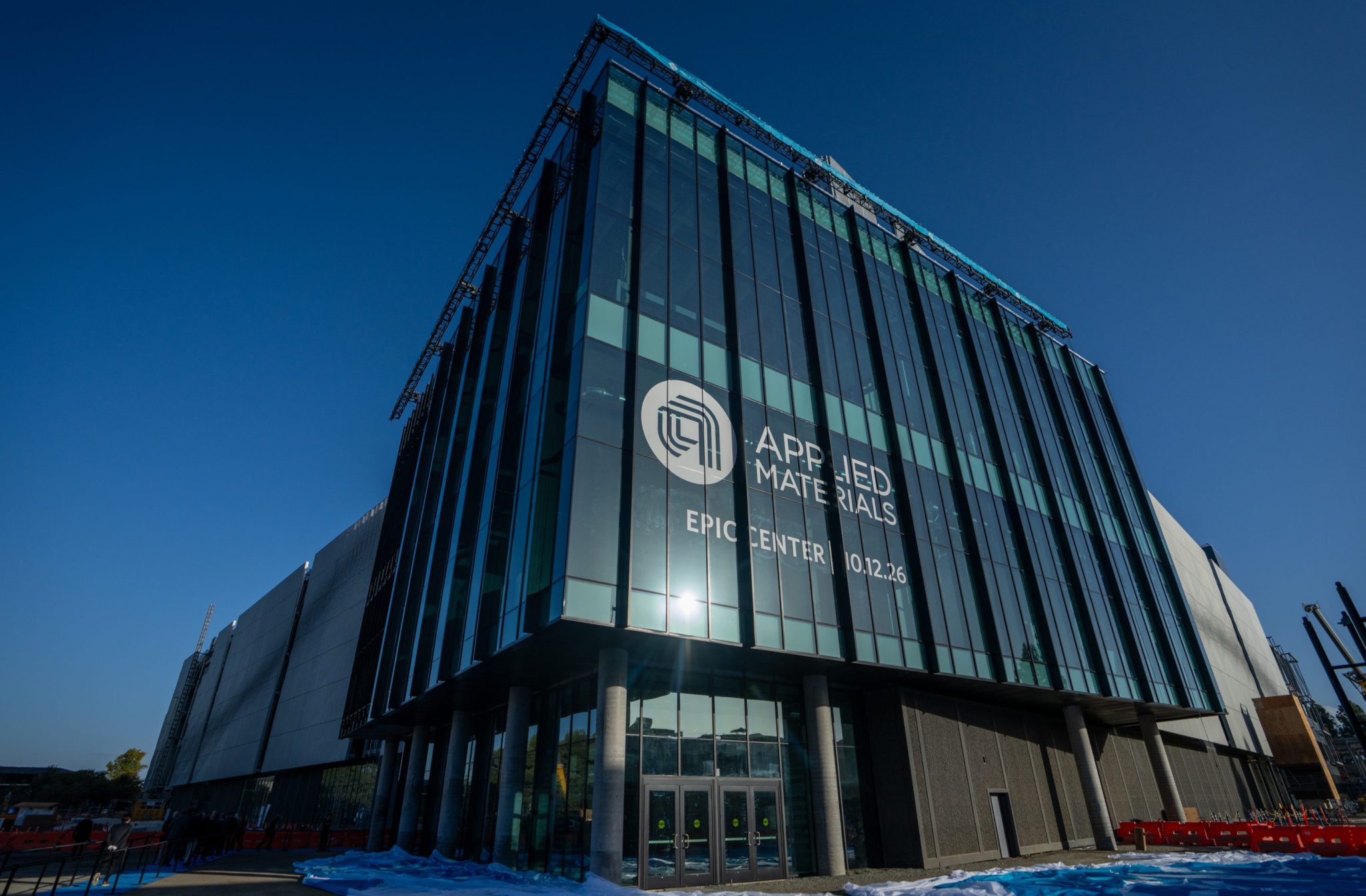
Applied Materials has opened a $5 billion Sunnyvale research centre with Intel, TSMC, Micron, SK Hynix and Samsung to speed chip design and development.
Follow the storyAI29 stories
01Summary
- 01Applied Materials unveiled its EPIC semiconductor research and development facility on Monday at its Sunnyvale, California campus.
- 02The 600,000-square-foot centre is a two-year construction project and is described by the company as the largest-ever US investment in advanced semiconductor equipment R&D.
- 03Applied says the collaboration could cut chip development time from 10 to 12 years to as little as six years.
- 04Partner companies include Intel, TSMC, Micron, SK Hynix and Samsung, with each having researchers on site.
- 05Applied Materials said the facility is for research only, not commercial chip production.
02Why it matters
The centre could help speed up the next generation of chips used in AI and memory, which matters for the pace of technology development. It also underlines how hard the US is trying to keep key semiconductor work closer to Silicon Valley.
Pulse AIAsk about this story
Answers are generated by AI from the story summary; they are not investment, health or legal advice.


